 Campus Walk
Atomic force microscopy (AFM)
The Veeco dimension 3100 AFM (AFM) is a magnification instrument capable of measuring the three-dimensional textures of a microscopic region with a horizontal and vertical resolution of a few nanometers. Utilized for mapping the topography of a thin layer with a maximum roughness of a few micrometers. The equipment measures the deflection caused by a sharp tip on a micron-sized cantilever as it scans across the specimen's surface. The instrument's handling range for sample sizes us 1 x 1 m.
Scanning Modes:
The AFM can scan in either Tapping or Contact Mode. Each mode should be selected based on the specimen to be scanned and the type of results desired. When working with a different sample, examine the AFM microscopy literature to identify which mode is most suited to your specific application.
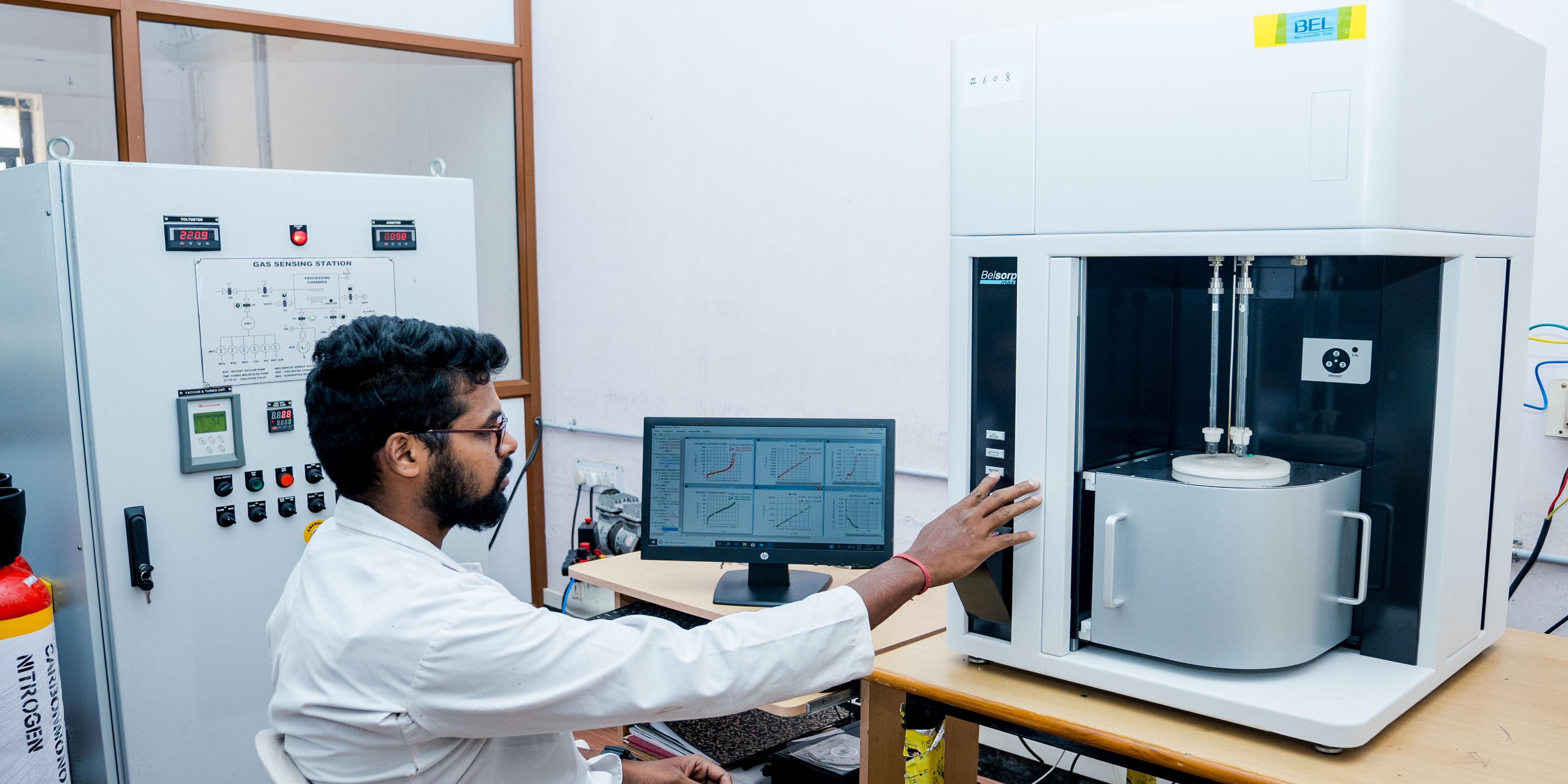
Bruner Emmet Teller (BET)- Surface area analyser
BET instrument is used to analysis porosity from micropore to mesopore and macropore by gas adsorption measurement of N2, Ar, CO2 and more. Low total surface area analysis with Kr at 77.4 K. High-quality, reproducible BET specific surface area (SSA) and pore size distribution (PSD) evaluation from an adsorption isotherm, starting from extremely low pressure. Making of BelshorpMax in JAPAN. Instrument in funded by UGC-SAP in 2019.
Dynamic Light Scattering (DLS)
The Litesizer Series instruments are designed for characterizing particles in liquid dispersions. The Litesizer 500 can determine Particle Size, Zeta Potential and Molecular mass by measuring Dynamic (DLS), Electrophoretic (ELS) and static light scattering (SLS) respectively it can also measure the sample transmittance. DLS is a non-invasive technique that measures the size and size distribution of small particles in a solution or suspension by analyzing their Brownian motion. The method is sensitive to particles ranging in size from 10 nm to 20,000 nm and can determine various properties of the particles, such as their Zeta Potential, stability, and molecular weight. Additionally, DLS can be used for both highly concentrated and highly dilute samples, making it a versatile analytical tool for many applications in various fields.
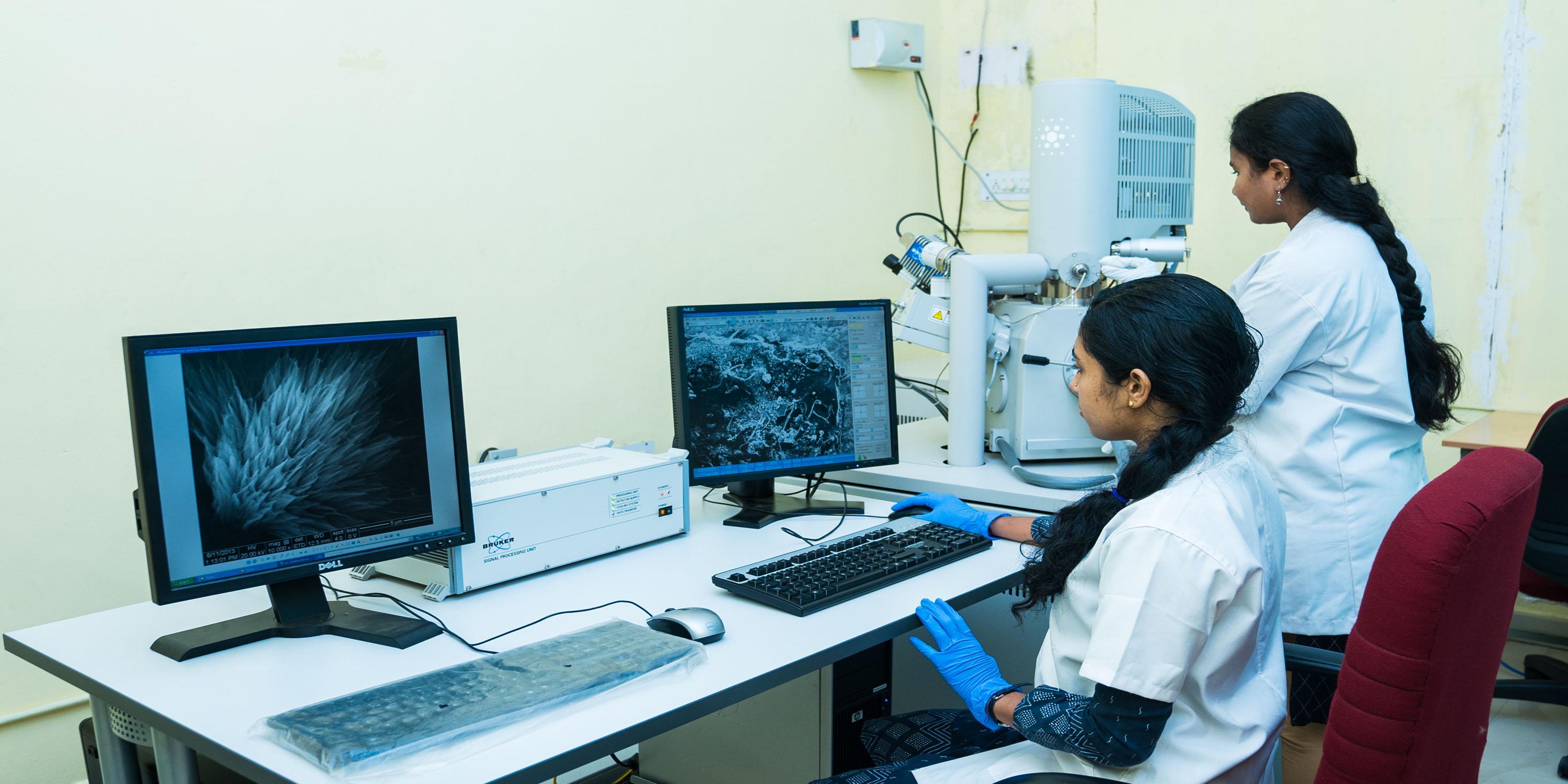
Field Emission Scanning Electron Microscopy (FESEM)
Make : FEI
Model : Quanta 250 FEG
Specification : Accelerating voltage 200V-30kV
: Operating Voltage 5-30kV
Magnification : 30X- 300kX Resolution : @30kV@High vacuum conditions: 1.2 nm : @30kV@Low vacuum conditions: 3.0 nm
- The FEI Quanta 250 FEG-SEM is equipped with schottky field emission gun and Everhart-thornley detector for (secondary electrons) to deliver ultrahigh resolution (1.2nm @ 30kV), backscattered electron detector in high vacuum mode and large field secondary electron detector for low vacuum operation (3.0nm @ 30kV) imaging.
- The Quanta 250 successfully integrates with EDAX detectors that make it ideal for: nanotechnology, material science, and biology, compositional and micro-structural imaging and analysis.
FTIR Spectrometer
The FT/IR-4600@ JASCO was designed to provide operational features and sensitivity levels found only in more expensive instruments. The innovative technology incorporated in these instruments results in exceptionally high signal-to-noise ratio specifications. The FT/IR-4600 offers exceptional flexibility and can be easily upgraded to meet new requirements. Optional expandability includes microanalysis with an FT-IR microscope, IR imaging with a multichannel microscope, and rapid scan option. The JASCO Quick Start System enables users of all experience levels to measure samples and perform data processing functions quickly and easily with a simple push of a button.
Features:
Wave number Extension: The FT/IR-4600 can mount two detectors inside of the main unit and then switch between them using software control. The standard working range, 7800 to 350 cm-1 (mid-infrared) can be modified to cover the NIR (15000 to 2200 cm-1) or Far-IR (5000 to 220 cm-1).
Excellent Signal to Noise Ratio: Featuring a highly stable interferometer and the AccTrac™ DSP technology providing consistent and accurate tracking of mirror position and velocity for optimum signal-to-noise performance.
Specifications:
Max resolution: 0.7cm-1
S/N ratio: 25,000:1
Photoluminescence spectroscopy
Model and manufacturer: Horiba FluoroMax 4L Spectroflurometer
The Horiba FluoroMax 4L spectrometer is a powerful tool for measuring fluorescence of, liquids, and thin films. The chemical structure of the substance is determined using the spectrofluorometer, which detects the radiation that an excited molecule emits. It may be applied to the quantitative estimation and qualitative analysis of emissive materials.
Measurement Modes for the FluorMax 4
- Fluorescence, Chemi-, bio- and electroluminescence
- Excitation, emission, synchronous scans
- Quantitation and analysis through Origin
Stylus profilometer
Bruker's Dektak® stylus profilers culminate over five decades of proprietary technology advances. They provide repeatable, reliable, and accurate measurements- from traditional step height measurements and 2D roughness surface characterization to advanced 3D mapping and film stress analyses. Dektak surface profilers have been widely accepted as the gold standard for measuring thin film thickness, stress, surface roughness, and form in diverse application areas from academic research to semiconductor process control.
Raman spectroscopy
Raman spectroscopy @ Horiba LabRAM HR probes the chemical structure of a material and provides information about:
- Chemical structure and identity
- Phase and polymorphism
- Intrinsic stress/strain
- Contamination and impurity
Typically, a Raman spectrum is a distinct chemical fingerprint for a particular molecule or material and can be used to very quickly identify the material, or distinguish it from others. Raman spectral libraries are often used to identify a material based on its Raman spectrum – libraries containing thousands of spectra are rapidly searched to find a match with the spectrum of the analyte.
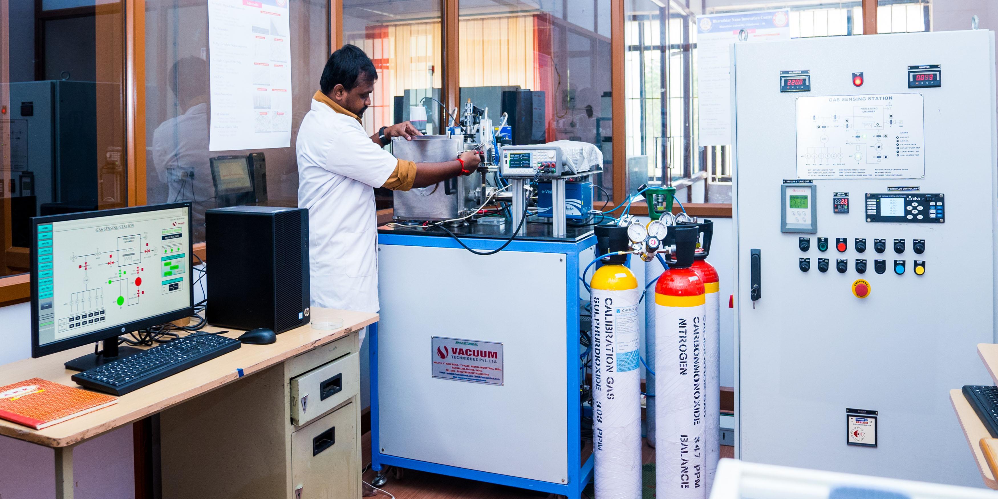
Solid State Impedance Analyzer
Solartron 1260A Impedance Analyzer is used to measure complex electrical impedance as a function of test frequency. Impedance analysis can also be used to characterize materials exhibiting dielectric behaviour of nanomaterials. Solid-state materials can exhibit complex electrical behavior due to their structure and properties, and impedance analysis can provide important information about their electrical properties, including resistance, capacitance, and inductance.
Impedance analyser comes in three distinct hardware implementations, and together these three implementations can probe from ultra-low frequency to ultra-high frequency and can measure impedances from µΩ to TΩ. This involves the phase sensitive measurement of current and voltage applied to a device under test while the measurement frequency is varied over the course of the measurement. Key specifications of an impedance analyzer are the frequency range, impedance range, absolute impedance accuracy and phase angle accuracy.
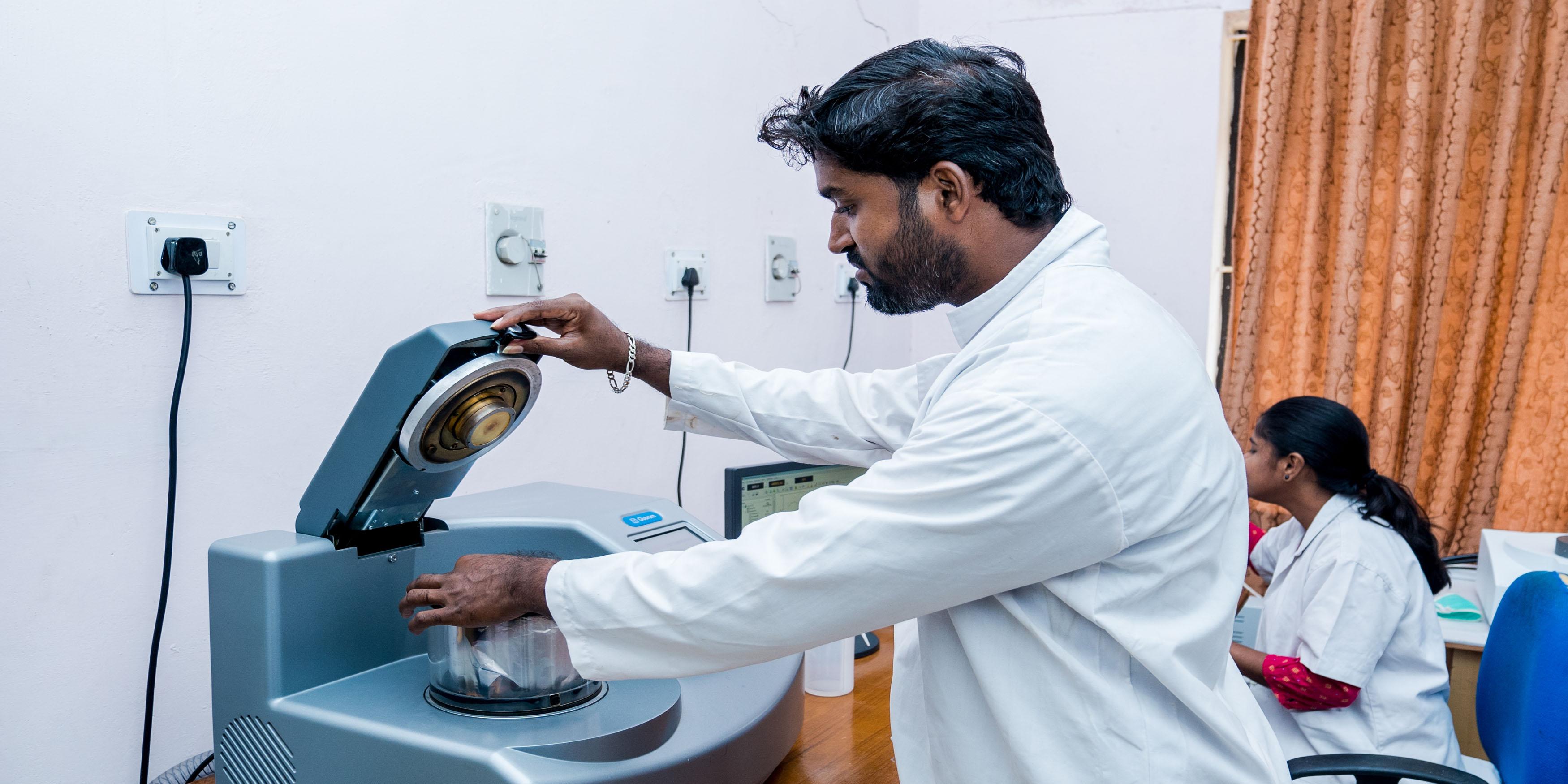
Thermal analyser (TGA)
The STA 8000 simultaneous thermal analyzer offers performance, reliability. It is a standard method to analyze organic, inorganic and synthetic materials. Thermogravimetric analysis in general means the measurement of the weight loss during a user-defined temperature or heating process. STA 8000 analysis TG with DTA mode and DSC (mW) mode for fast enhanced result interpretation. It has wide temperature range measurements from room temperature to 1000 °C with superior accuracy and sensitivity. Vertical displacement balance sensor (not rotational) provides weight insensitivity to sample position, e.g., no spurious weight change from melting.
UV-visible spectrometer
The Jasco V-650 Spectrometer is a double-beam spectrophotometer with a photomultiplier tube detector. The high sensitivity of the photomultiplier tube detector enables accurate measurements of low concentration samples. By controlling the high voltage applied to the PM tube, the dynode feedback circuit allows a wider dynamic range. It also enables the use of such solid/liquid sample handling accessories as integrating spheres to collect diffuse light transmitted or reflected by the sample. Advanced optical design that results in high optical throughput as well as allows bandwidth to be set as low as 0.1 nm for high resolution work. Spectra Manager software, the latest version of JASCO's innovative cross-platform spectroscopy software.
UV-visible spectrometer is a powerful analytical tool that is used in a wide range of applications, including:
Analysis of organic molecules: UV-visible spectrometer is used to determine the concentration of organic molecules, such as proteins, nucleic acids, and drugs, in solution. These molecules absorb UV-visible light in specific regions of the spectrum, and the amount of light absorbed is proportional to the concentration of the molecule.
Material characterization: UV-visible spectrometry is used to study the electronic properties of materials, such as semiconductors and catalysts. The absorption or transmission of UV-visible light can provide information about the electronic structure of the material, which can be used to optimize its performance in various applications.
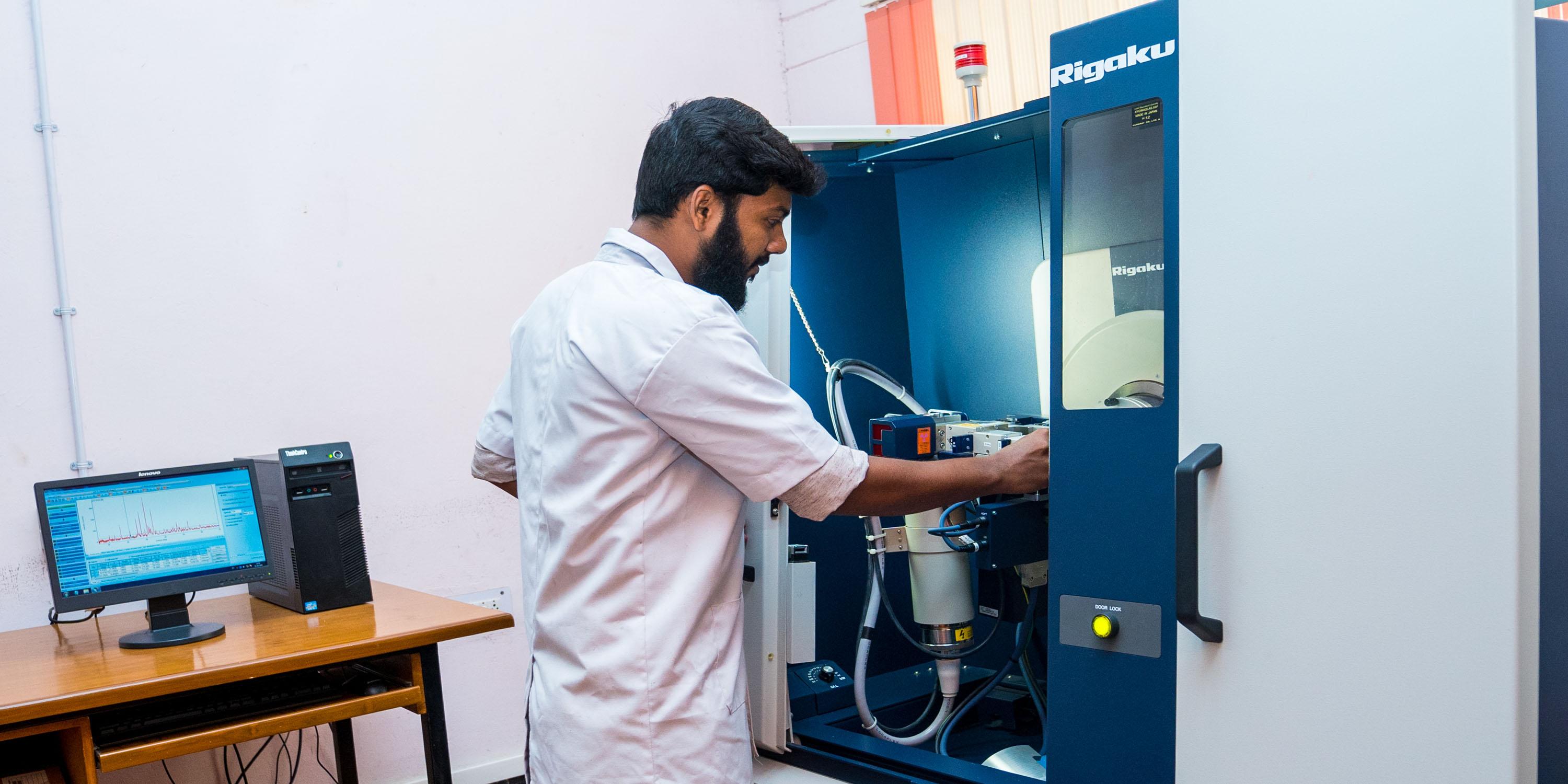
X-Ray diffraction analysis (XRD)
XRD has been used extensively for the examination of nanomaterials and thin films. Rigaku Utima IV XRD installed in the year 2016 under DST FIST program. Individual experiments are optimized with accessories like the D/teX Ultra high-speed position sensitive detector system and thin film attachment incorporating Rigaku's patented cross beam optics (CBO) technology for permanently mounted, permanently aligned and user-selectable parallel and focusing geometries.
X-Ray diffraction analysis (XRD) has been used extensively for the examination of nanomaterials and thin films. XRD is a nondestructive technique that provides detailed information about the crystallographic structure, chemical composition, and physical properties of a material. Each phase of the material produces a unique diffraction pattern due to the material's specific chemistry and atomic arrangement. The generated X-rays are collimated and directed to a nanomaterial sample, where the interaction of the incident rays with the sample produces a diffracted ray, which is then detected, processed, and counted. The intensity of the diffracted rays scattered at different angles of material are plotted to display a diffraction pattern.